SoftSSD-Platform
Hardware Architecture
Our SSD development platform is built around the Xilinx Zynq® UltraScale+™ MPSoC as the core board. This device features a heterogeneous computing architecture, integrating programmable ARM Cortex® application processors with a high-performance FPGA fabric on a single chip. This combination enables flexible and efficient execution of both control-plane tasks (on the ARM cores) and data-plane acceleration (in the FPGA logic).
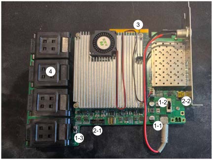
The core board is mounted onto a custom carrier (or base) board, which provides essential system-level support, including:
- Power delivery and regulation (1-1 12V DC power, 1-2 On/Off control, 1-3 Voltage control),
- Debug interfaces (2-1 JTAG, 2-2 UART),
- A PCIe interface for host connectivity (3), and
- NAND flash interfaces to connect multiple flash packages (4).
APU and RPU
- ARM application processors: High-performance ARM cores (quad-core Cortex-A53) to handle application-level tasks.
- Co-processors: Auxiliary processing units, Cortex-R5 real-time cores (used for real-time control, safety-critical tasks, or low-latency I/O), that assist the main application processors.
The SSD firmware runs on the ARM application processors, while flash translation and ECC offload are handled by dedicated co-processors.
FPGA
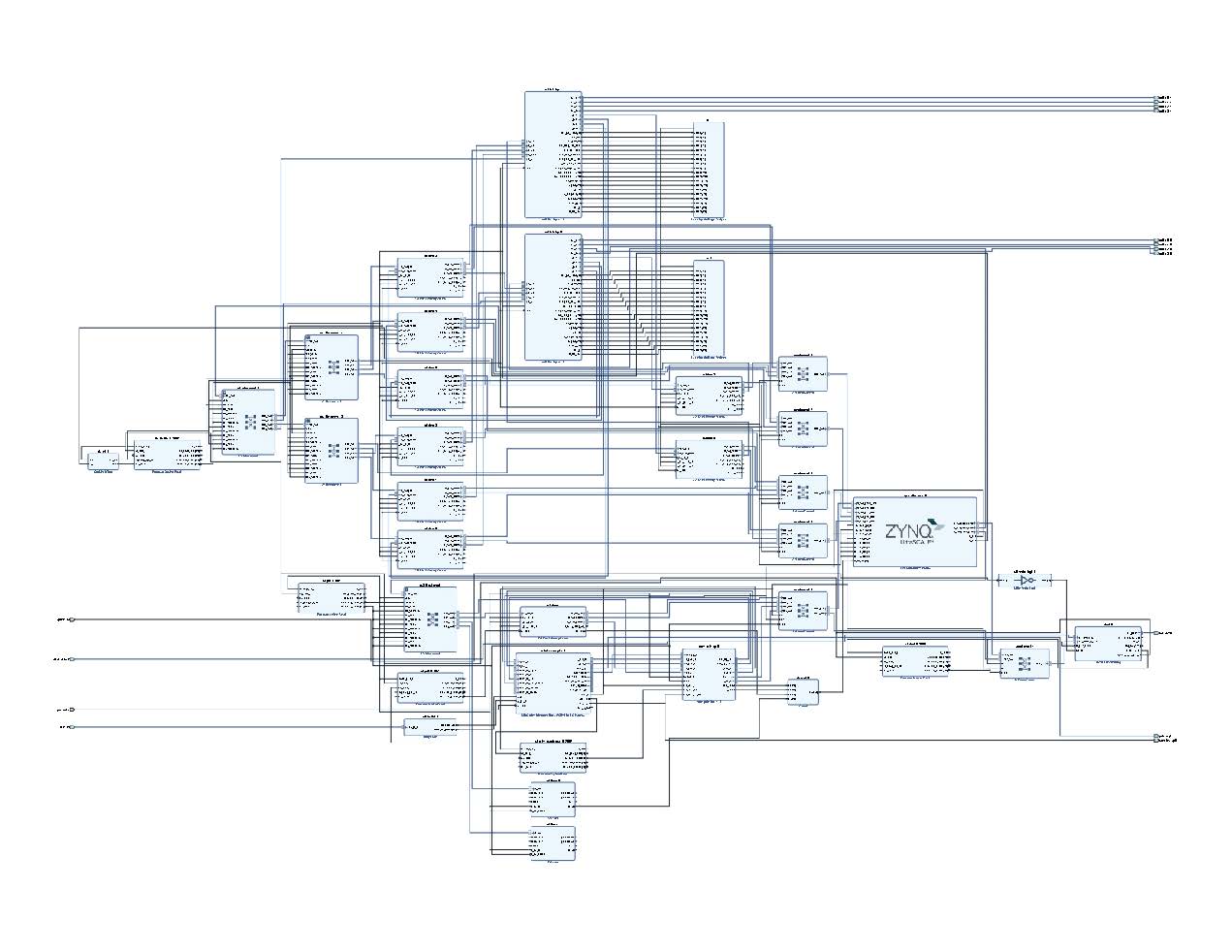
The FPGA implements a NVMe-over-PCIe controller and ONFI-compliant NAND flash controllers. These controllers are connected with both on-board DDR memory and the ARM processor’s memory hierarchy, enabling efficient data movement across the heterogeneous compute fabric.
-
The NVMe-PCIe controller handles host communication via the PCIe interface, managing Submission and Completion Queues and performing DMA operations.
-
The ONFI flash controller manages low-level NAND operations, including read, program, and erase commands, timing control, and interface protocol compliance. Each flash controller corresponds to one flash memory channel, and the system currently supports up to eight channels.
Memory Regions
The SSD board has three physical memroy regions:
- PL DDR (4GB): Data cache
- PS DDR Low (2GB): L2P mapping cache and Flash transaction buffer
- PS DDR High (2GB): L2P mapping cache
Flash Memory
Pins on the FPGA have been assigned for the flash chip interface, supporting up to 8 channels. Regarding interface protocols, NV-DDR2 is currently stably supported, while NV-DDR3 is supported experimentally. The board is shipped with the following flash chips:
- MLC NAND chip: MT29F1T08CUCCB (2 channels per package)
- TLC NAND chip: MT29F512G08EBHBF (1 channel per package) In theory, other flash chips with compatible interface protocols can be substituted, provided that pin assignments are correctly configured accordingly.
The performance of pages at different locations within TLC NAND flash varies significantly. To provide a reference, internal bandwidth measurements for the SSD platform employing TLC chips (MT29F512G08EBHBF) are summarized in the table below: |Page latecncy|Lower-page|Upper-page|Extra-page|avg.| |—|—|—|—|—| |read|115us|130us|145us|130us| |program|600us|60us|1460us|706us|
| Internal bandwidth | Per-channel (single die) | Overall |
|---|---|---|
| read | 120MB/s | 480MB/s |
| program | 20MB/s | 80MB/s |
The FPGA operates at a frequency of 200 MHz and is configured to match the timing mode 7 of NV-DDR2/3. Each channel employs an 8-bit wide differential signaling interface, transferring data on both the rising and falling edges of the clock. Consequently, the theoretical bandwidth per channel is 400 MB/s.
All dies within a channel time-share the channel’s bandwidth. By increasing the number of LUNs (dies) per channel and leveraging interleaved die access (multi-LUN) along with multi-plane read/write operations, the effective bandwidth can approach this theoretical limit.
Under ideal conditions, with all eight channels operating simultaneously, the aggregate bandwidth ceiling reaches 3.2 GB/s.